





Optical-Grade Monocrystalline Silicon Ingots
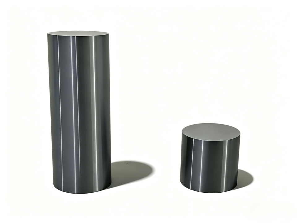
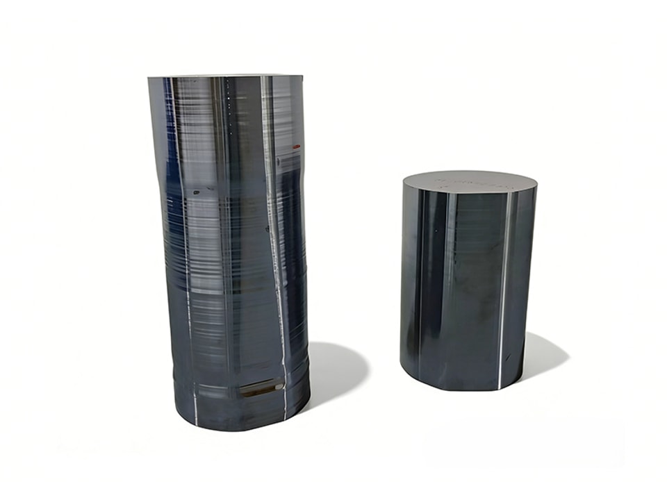
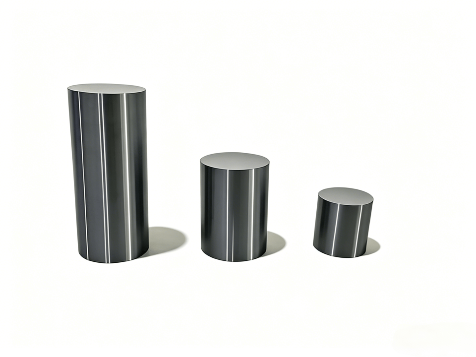
Optical-Grade Monocrystalline Silicon Ingots
Optical-Grade Silicon for Infrared and Photonics Applications
Optical-grade monocrystalline silicon ingots are high-purity silicon materials designed for infrared optics, optoelectronic devices, silicon photonics and advanced sensing systems. With excellent crystal uniformity, stable electrical properties and reliable optical performance in infrared wavelength ranges, monocrystalline silicon provides a critical material foundation for high-precision optical and semiconductor applications.
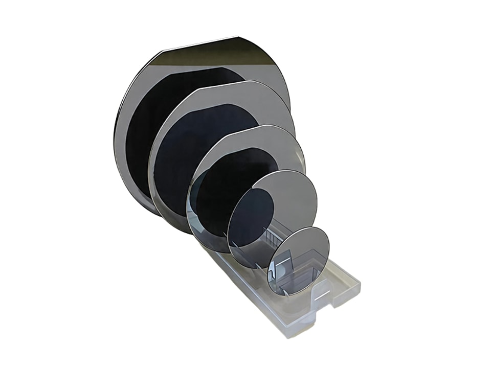
These ingots can be sliced and processed into wafers or optical components according to customer requirements, supporting applications in infrared sensing, laser ranging, silicon photonics, MEMS devices and high-performance semiconductor systems.
Key Advantages
- Excellent infrared optical performance for mid-wave and long-wave infrared applications.
- High crystal integrity for stable optical and electrical performance.
- Customizable resistivity, conduction type, crystal orientation and dopant selection.
- Compatibility with semiconductor wafer processing and microfabrication.
- Suitable for infrared sensors, photodetectors, MEMS structures and silicon photonics devices.
Application Areas
Infrared Optoelectronic Devices
Monocrystalline silicon is widely used in infrared optoelectronic applications due to its excellent optical properties in key infrared wavelength ranges. It is suitable for high-end infrared optical systems, infrared sensing modules and precision optical components.
Silicon Photonics
In silicon photonics, monocrystalline silicon can be used to build silicon-based waveguides, modulators and grating couplers, enabling high-speed optical interconnection in data centers and communication systems. By replacing traditional electrical signal transmission with optical signal transmission, silicon photonics helps improve bandwidth, reduce latency and enhance energy efficiency.
Silicon-Based Photodetectors
Based on its carrier mobility and semiconductor characteristics, monocrystalline silicon can support high-speed and high-sensitivity photoelectric signal conversion. It is widely used in laser ranging, optical sensing and near-infrared detection systems.
MEMS Optical and Automotive Sensors
Monocrystalline silicon also serves as an ideal substrate for MEMS devices because of its high elastic modulus, low fatigue characteristics and anisotropic crystal structure. Through microfabrication processes such as DRIE, silicon can be processed into accelerometers, pressure sensors, gyroscopes and micro-mirrors used in automotive safety systems, LiDAR and precision sensing applications.
LiDAR Micro-Mirrors
Using the mechanical elasticity of monocrystalline silicon, MEMS micro-mirrors can achieve high-frequency laser beam steering for compact automotive LiDAR and three-dimensional sensing systems.
Custom Specifications Available
Sispread can customize optical-grade monocrystalline silicon ingots according to customer requirements, including size, resistivity range, conduction type, crystal orientation and dopant selection. Special specifications are available upon request for infrared optical systems, silicon photonics platforms and advanced sensor manufacturing.
| Parameter | Specification |
|---|---|
| Product Name | Optical-grade monocrystalline silicon ingots |
| Size | 4 inch, 5 inch, 6 inch, 8 inch; custom sizes available upon request |
| Resistivity Range | Customizable according to customer requirements |
| Conduction Type | N-type, P-type |
| Crystal Orientation | <100>, <111>; special crystal orientations available upon request |
| Dopant | N-type: Phosphorus (P), Arsenic (As), Antimony (Sb); P-type: Boron (B) |
Related Products

Sispread supplies high-purity monocrystalline silicon ingots, silicon wafers and semiconductor silicon materials for global manufacturing customers.
- AddressNo.159 Mudanjiang Road, Rudong Economic Development Zone, Jiangsu Province, China
- EmailSispread@sispread.com
- Phone+86 513 81907550


Copyright © 2022-2026 Jiangsu Sispread Semiconductor Materials Co., Ltd. All Rights Reserved.
We use cookies and analytics to improve website performance and understand visitor behavior. By continuing to browse, you agree to our Privacy Policy.