


.jpg")

Company Profile
Jiangsu Sispread Semiconductor Materials Co., Ltd. (hereinafter referred to as “Jiangsu Sispread”) was established in November 2022.It is a technology enterprise specialising in semiconductor-grade Czochralski monocrystalline silicon products, focusing on the research and development, production...
Products
READ MORE >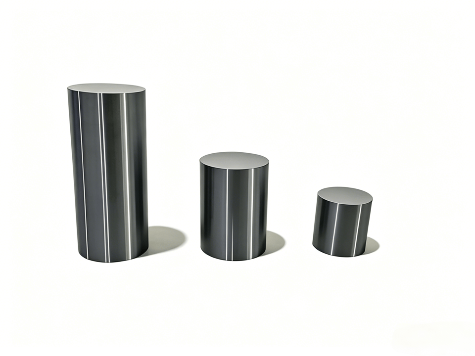
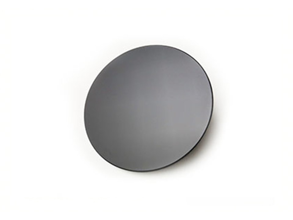
Optical-grade monocrystalline silicon ingots
| Material | Monocrystalline Silicon |
|---|---|
| Purity | ≥ 99.9999986% |
| Application | Optical Components |
| Diameter | Customizable |
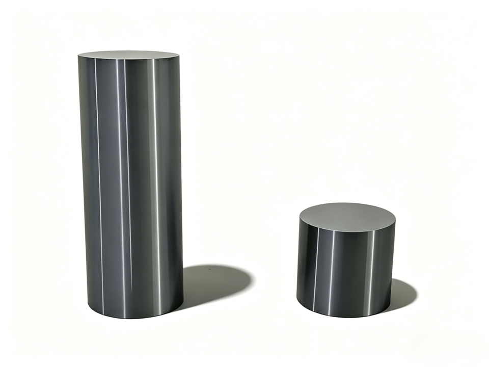
Electronics-grade monocrystalline silicon ingots
| Material | Electronic Grade Silicon |
|---|---|
| Resistivity | 0.1 - 100 Ω·cm |
| Type | N-Type / P-Type |
| Orientation | <100> / <111> |
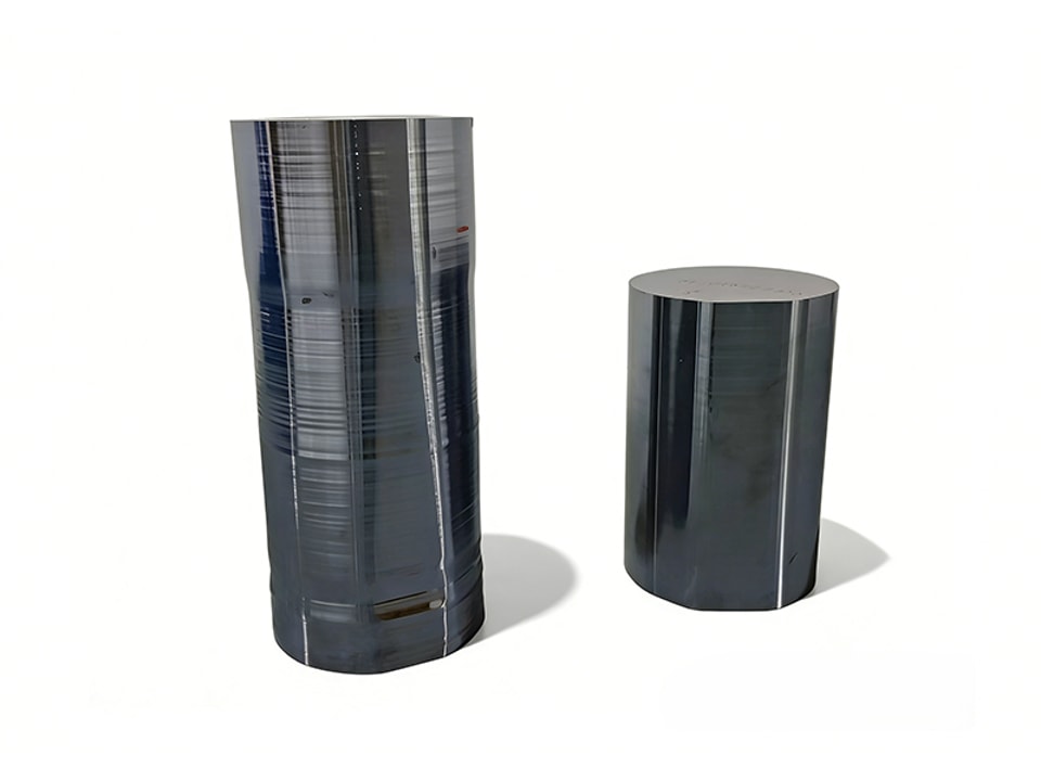
Monocrystalline silicon ingots (rough ingots)
| State | Rough Ingot |
|---|---|
| Conductivity | P/N Type available |
| Crystal Structure | Monocrystalline |
| Length | Up to 2000mm |
Silicon wafer
| Product Type | Polishing & Grinding Tool |
|---|---|
| Material Compatibility | Silicon, Quartz, Glass |
| Durability | High Wear Resistance |
| Dimensions | Standard & Custom |
Our Advantage
The truths we least like to hear are those which it is most to our advantage to know.
Professional Track
Focus on 4–8 inch semiconductor-grade Czochralski monocrystals (As, Sb, P contained), meeting the needs of IC and power device fields.
R&D Strengt
Experienced R&D team, master key processes, with multiple proprietary intellectual property rights and continuous innovation.
Customized Solutions
Market-oriented, providing tailored solutions for different downstream scenarios, covering the whole service chain.
Quality & Reputation
Lean manufacturing ensures high quality; trusted by customers, actively expanding domestic and international markets.
This is NEWS
Jingsheng Electromechanical signs strategic cooperation agreement with Zhejiang University and Zhejiang Chuangxin to layout the integrated circuit industry
On June 24, 2025, Jingsheng Electromechanical, the School of Integrated Circuits at Zhejiang University, and Zhejiang Chuangxin signed a strategic cooperation agreement to jointly build two centers: the Advanced Integrated Circuit Equipment and Process Joint Research and Development Center, and the Integrated Circuit Talent Training and Technology Innovation School Enterprise Collaboration Center, to accelerate the breakthrough of domestic integrated circuit equipment through the integration of industry, academia, and research. Three parties focus on joint research and development of 12 inch silicon epitaxial equipment and processes, establish a talent attraction and education mechanism, and promote the integration of industry and education; Integrating the advantages of Jingsheng Electromechanical Industrialization, Zhejiang University Scientific Research, and Zhejiang Chuangxin Platform Transformation, we aim to build a closed loop of "basic research - technological breakthroughs - achievement transformation - industrial application", break through equipment bottleneck technology, cultivate composite talents, and enhance the core competitiveness of the industry. Jingsheng Electromechanical is a leading semiconductor material equipment company in China, with strong research capabilities in the School of Integrated Circuits at Zhejiang University and a provincial-level 12 inch integrated circuit innovation platform operated by Zhejiang Chuangxin; Previously, Jingsheng had led the Yangtze River Delta Silicon Wafer Polishing Technology Consortium. This cooperation further promotes equipment localization, cost reduction and efficiency improvement (expected to reduce costs by about 20%), and helps the domestic integrated circuit industry chain to be independently controllable.
Tiancheng Semiconductor makes a new breakthrough in 12 inch SiC
In October 2025, Tiancheng Semiconductor announced a major breakthrough in the research and development of 12 inch silicon carbide. Relying on self-developed long crystal equipment, it successfully produced high-purity semi insulating and N-type 12 inch SiC single crystals. The effective thickness of N-type crystals exceeded 35mm, and the self-developed equipment can produce a maximum of 350mm single crystals. At the same time, it has mastered the mature preparation process of two types of single crystals. The enterprise was established in 2021, deeply engaged in the research and development and manufacturing of silicon carbide substrates and long crystal equipment, with a clear pace of technological iteration: achieving small batch production of 6-inch SiC ingots by 2022; Breakthrough 8-inch technology by 2023; By 2024, achieve 8-inch mass production with thickness uniformity error controlled within 2 microns. By July 2025, we have taken the lead in conquering the core process of 12 inch N-type SiC, innovating the resistance furnace process to break through the bottleneck of growth rate in the industry, significantly reducing the density of microtubes, and achieving a yield rate of 65%. At present, the company has established a complete production line from single crystal furnace, powder preparation to large-scale crystal growth and processing, achieving independent and controllable SiC full process technology, and consolidating the core competitiveness of the localization of third-generation semiconductor substrates
Shanghai Hejing adds large-sized semiconductor silicon wafers
Recently, the domestic semiconductor silicon material field has ushered in an important layout. A research silicon investment of 400 million yuan has been made to build a large-scale semiconductor silicon single crystal base in Baotou. After completion, the annual production of single crystal silicon will exceed 1000 tons, and it is expected to be effective by December 2027; Shanghai Hejing plans to raise no more than 900 million yuan in additional funds, with a focus on investing in the industrialization of 12 inch large silicon wafers to assist in domestic substitution. The current global semiconductor silicon wafer market is dominated by an oligopoly, with the five major players accounting for about 90% and accelerating advanced card positioning processes. China is currently in a critical period of domestic substitution, and enterprises such as Shanghai Silicon Industry are promoting large-scale output with breakthroughs. Industry insiders say that the industry has high barriers and long cycles, and domestic companies' efforts to optimize their layout with international giants will intensify competition. The process of domestic substitution will promote the high-quality development of related industries in China