






Silicon wafer
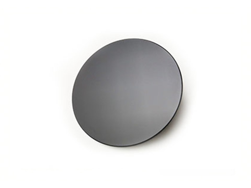
Silicon Wafer
Silicon wafers are precision-processed semiconductor substrates produced from high-quality monocrystalline silicon ingots. They provide the material foundation for integrated circuits, power semiconductor devices, MEMS sensors, photovoltaic cells and optoelectronic components.
With controlled crystal orientation, conduction type, dopant selection and surface quality, silicon wafers support downstream fabrication processes such as photolithography, thin-film deposition, ion implantation, etching and device packaging.
Silicon Wafers for Semiconductor, Power and Optoelectronic Devices
Silicon wafers act as the precision substrate for modern device manufacturing. Their crystal uniformity, controlled doping and surface quality enable reliable downstream processing across integrated circuits, power electronics, MEMS sensors and optoelectronic applications.
Why Monocrystalline Silicon Wafers Matter
After slicing, grinding, polishing and cleaning, silicon wafers provide a stable platform for photolithography, thin-film deposition, ion implantation and etching. A highly ordered crystal lattice helps maintain carrier mobility, device consistency and long-term reliability.
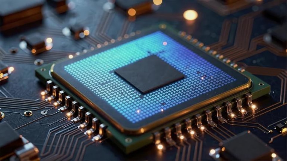
Integrated Circuits
Used as the substrate for logic chips, CPUs, SoCs and other IC devices that require stable crystal quality and precise process compatibility.
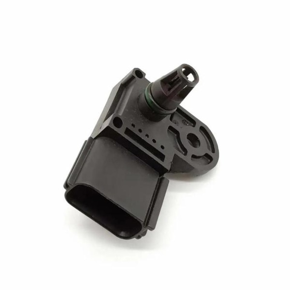
Power Semiconductor Devices
Support the manufacturing of IGBTs, MOSFETs and high-power diodes, where material consistency directly affects electrical performance.
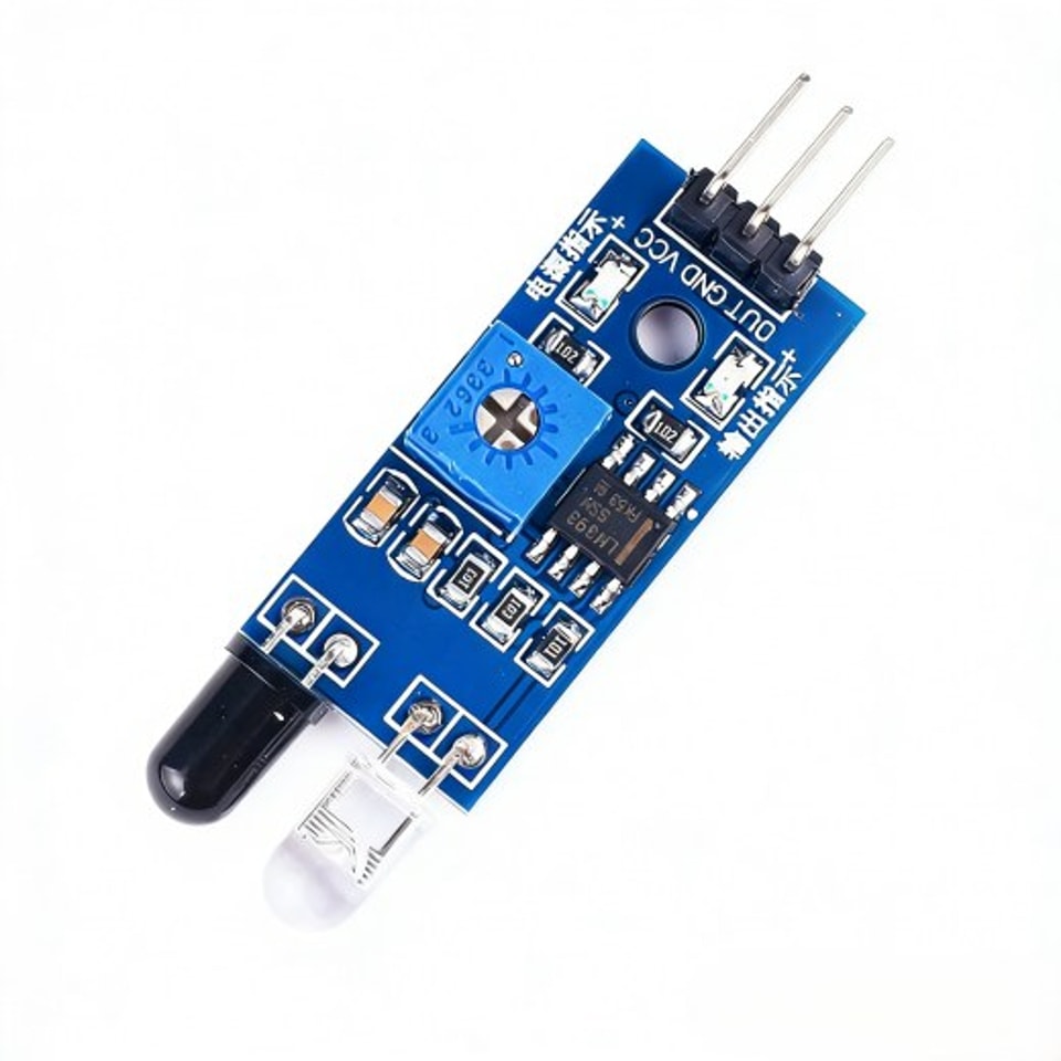
CMOS Sensors & MEMS
Provide precision substrates for CMOS image sensors, MEMS sensors and micro-structured devices used in automotive and industrial systems.
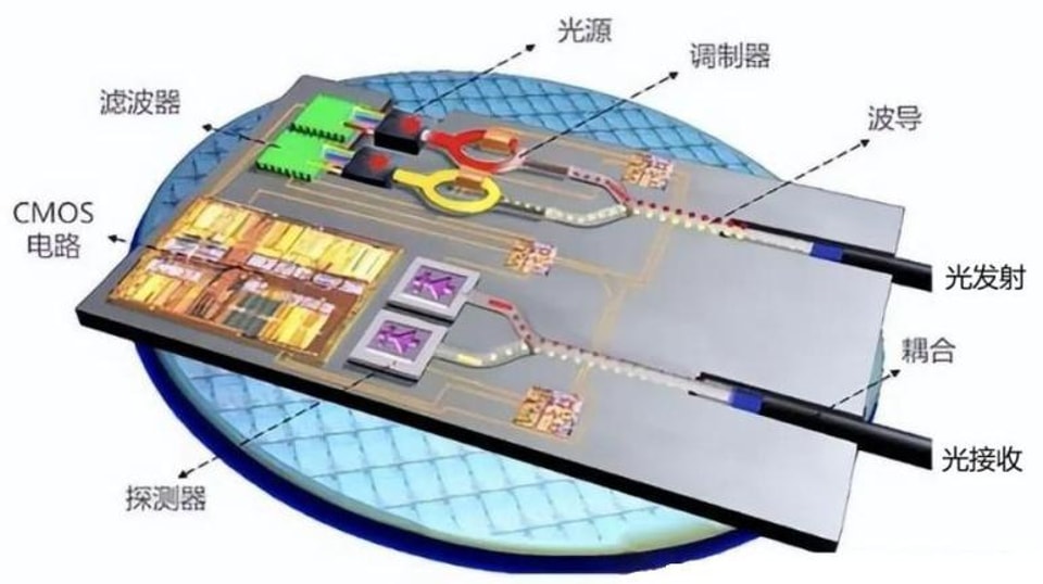
Optoelectronics & Photonics
Suitable for downstream optoelectronic components, photodetectors and silicon photonics platforms after precision processing.
Explore Sispread’s capabilities in one document
Review our company profile, crystal growth capacity, quality system and product portfolio for monocrystalline silicon ingots and silicon wafers.